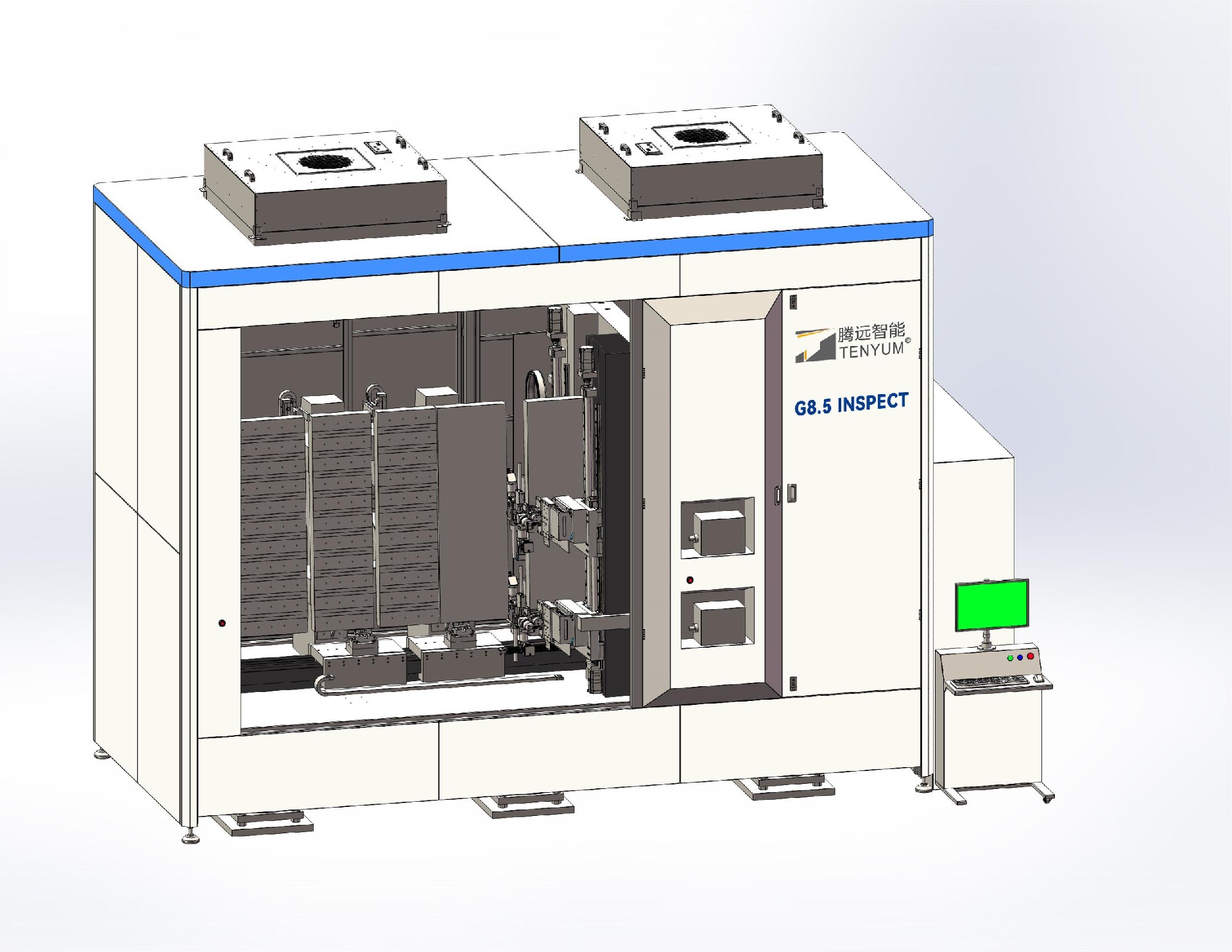
Inspection Equipment

300mm Wafer Defect Inspection System is a fully automated, high-precision defect inspection equipment that designed for 300mm and smaller wafers. It targets surface defects—such as line breaks, pattern errors, missing fill structures, glass damage, particles, and scratches—on patterned wafers, unpatterned wafers, and E-test areas.
The system adopts a modular design, with core components including a high-precision inspection platform and vision system, an automated wafer handling mechanism, and computer software algorithm development. Using a composite defect inspection system based on bright-field and dark-field imaging, it captures multi-dimensional images and employs deep learning algorithms to automatically classify and quantitatively analyze defects, meeting technical requirements for 300mm and sub-300mm wafer defect inspection.
l Compatible with 8-12 inch wafer with standard FOUP, SMIF;
l Supports patterned wafer defect inspection, unpatterned wafer defect inspection, and E-test area re-inspection;
l 300mm optical bright field + dark field composite defect inspection system(online);
l WDI auto-focus tracking system ensures defect capture rate ≥90%;
l Compatible with automated wafer loading/unloading and AGV docking for autonomous material handling;
l Customizable secondary development software with an intuitive and user-friendly interface.
By utilizing broad-spectrum illumination from deep ultraviolet to visible wavelengths or high-power deep UV single-wavelength laser lighting, combined with high-resolution, large-field-of-view optical bright-field or dark-field imaging methods, the system captures circuit pattern images from wafer surfaces. It enables real-time pattern alignment and analysis, along with defect identification and classification, to achieve accurate capture of pattern defects on wafers.
Standard Pattern Defect Inspection
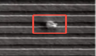
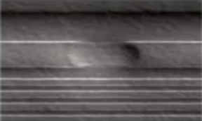
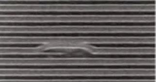
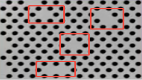
Targeting patterned wafers post-lithography, un-patterned wafers, and complex logic chip patterns, it detects defects including line breaks, pattern errors, missing fill structures, glass damage, particles, and scratches.
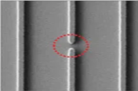
Edge Breakage and crack inspection after dicing
Inspect chip edge breakage, crack, chip loss and other defects after dicing.
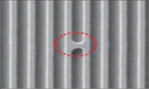
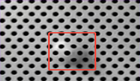
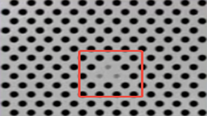
Bump Defect Inspection
Bump anomalies such as diameter, height, brightness, loss and bridging can be detected through 2D and 3D detector.

 +86 0731-8487 7386
 info@tenyum.com
 Building 4, Haodan Science Park, Furong District,


 微信扫一扫
微信扫一扫