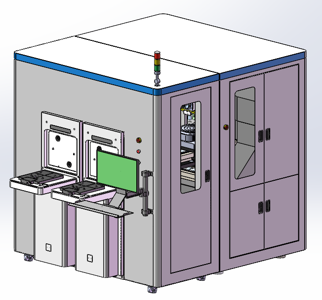
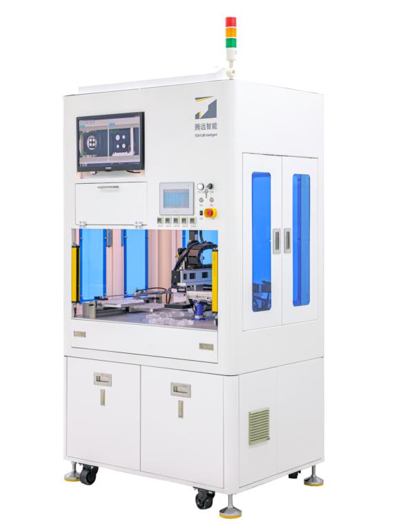
Inspection Equipment
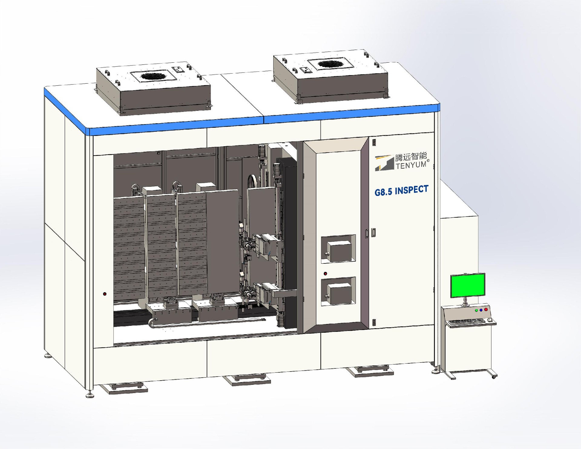
The G8.5 Photomask Inspection System is a defect inspection equipment developed for large-size mask substrates/blank in the semiconductor/FPD industries. It is designed to high accuracy identify micron defects such as particles, pinholes, scratches, edge chipping, stains, and pattern errors in mask substrates/Blank. The system adopts a modular design, with core components including a high-precision air bearing table and control system, vibration isolation airbag system, high-precision marble platform, multi-magnification microscopic imaging optical system, and computer control system. The inspection process is based on three optical modes—bright field, dark field, and transmission—to capture multi-dimensional images, and automatically classifies and quantifies defects through deep learning algorithms, meeting the technical requirements for mask substrates and mask accuracy of advanced processes of G8.5 generation lines and below.
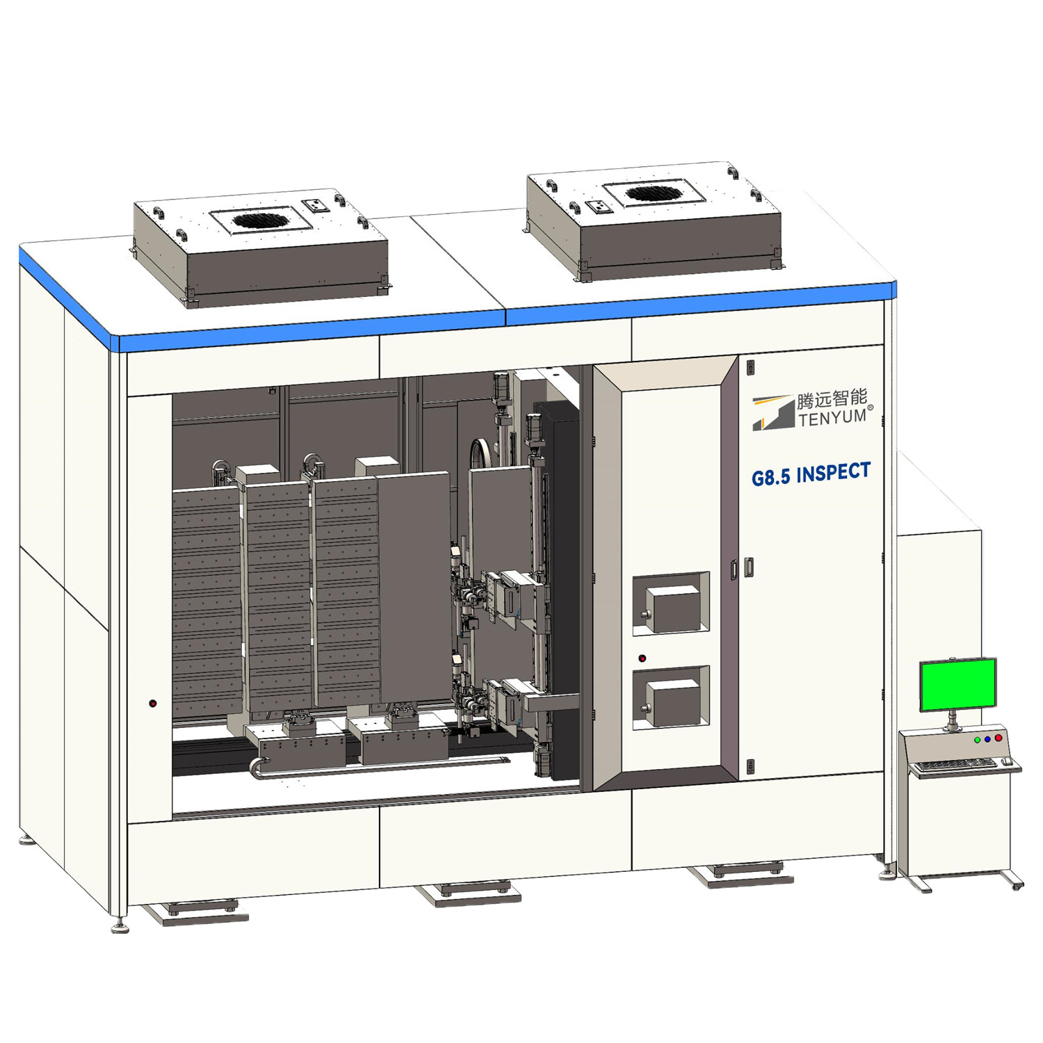
l Support a maximum size of 8.5 generation TFT masks (Customized for 8.6-10.5 generation mask).
l Support vertical stage (Customized for horizontal stage).
l Support multiple optical lenses scanning greatly improves inspection efficiency.
l High-efficiency microscopic tracking system ensures image quality under large-area imaging.
l Support automatic loading and unloading, support interconnecting with AGV.
l Customized directional secondary development software with clear and easy operation interface.
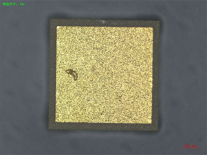
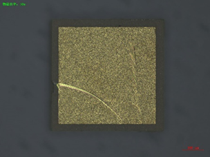
For large-sized mask substrates, high-precision CCD camera systems are employed to capture images for the detection of surface defects such as particles, pinholes, scratches, protrusions, and depressions. The captured images are then processed via an image processing card and computer software systems using a series of algorithms.
Subsequently, the processed images are compared against standard reference images
to identify defects and generate inspection reports.

l Blank substrate manufacturing, process control for large-sized mask substrates;
l Defect inspection requirements for mask substrates used in optical and lithography applications;
l Defect inspection during the glass substrate/mask Blank manufacturing.

 +86 0731-8487 7386
 info@tenyum.com
 Building 4, Haodan Science Park, Furong District,


 微信扫一扫
微信扫一扫